UV Exposure Unit

Sept. 10, 2015 - Nov. 16, 2015

Mobirise
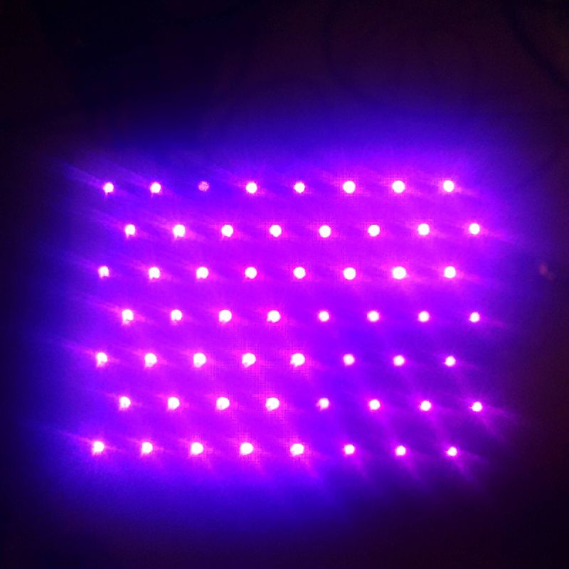
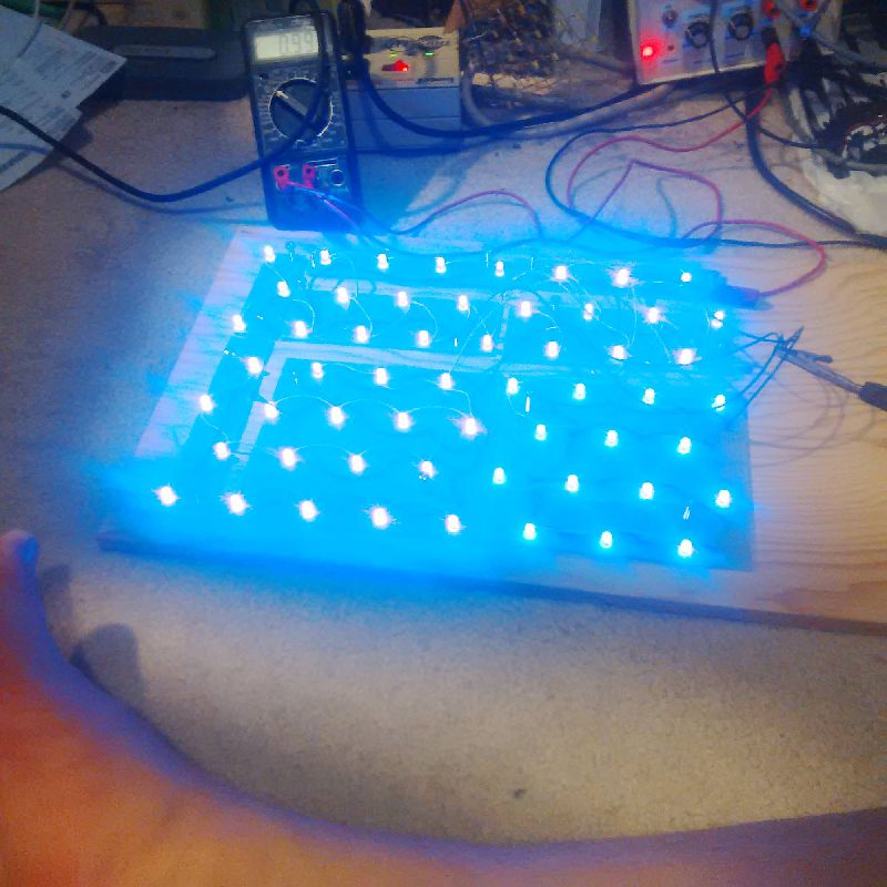
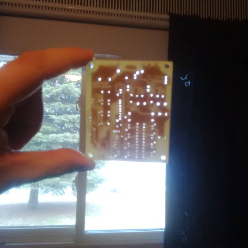
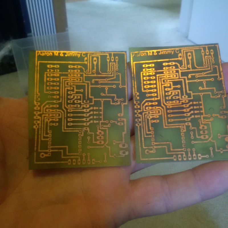
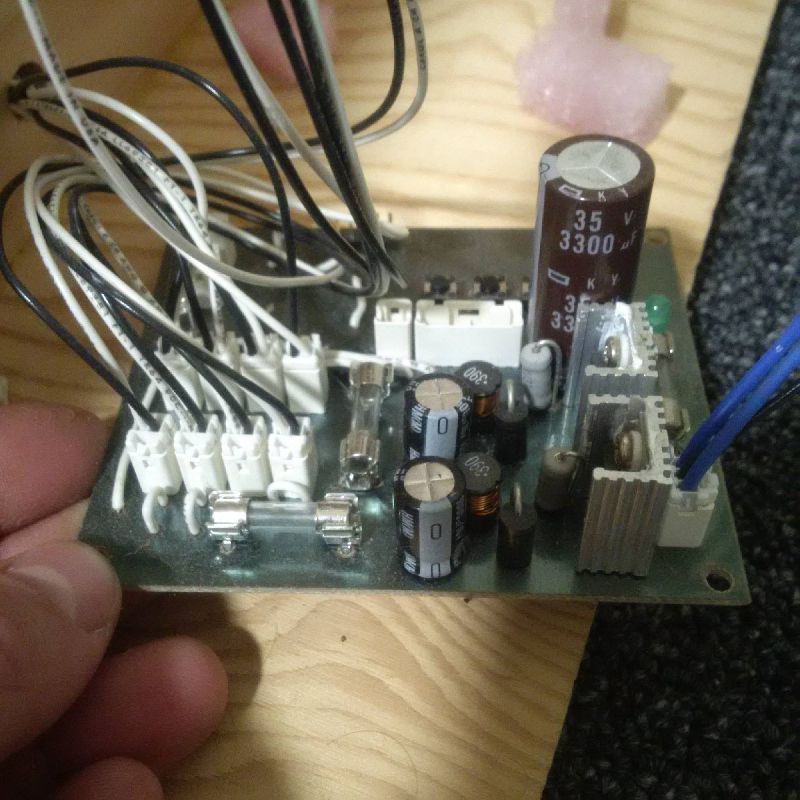
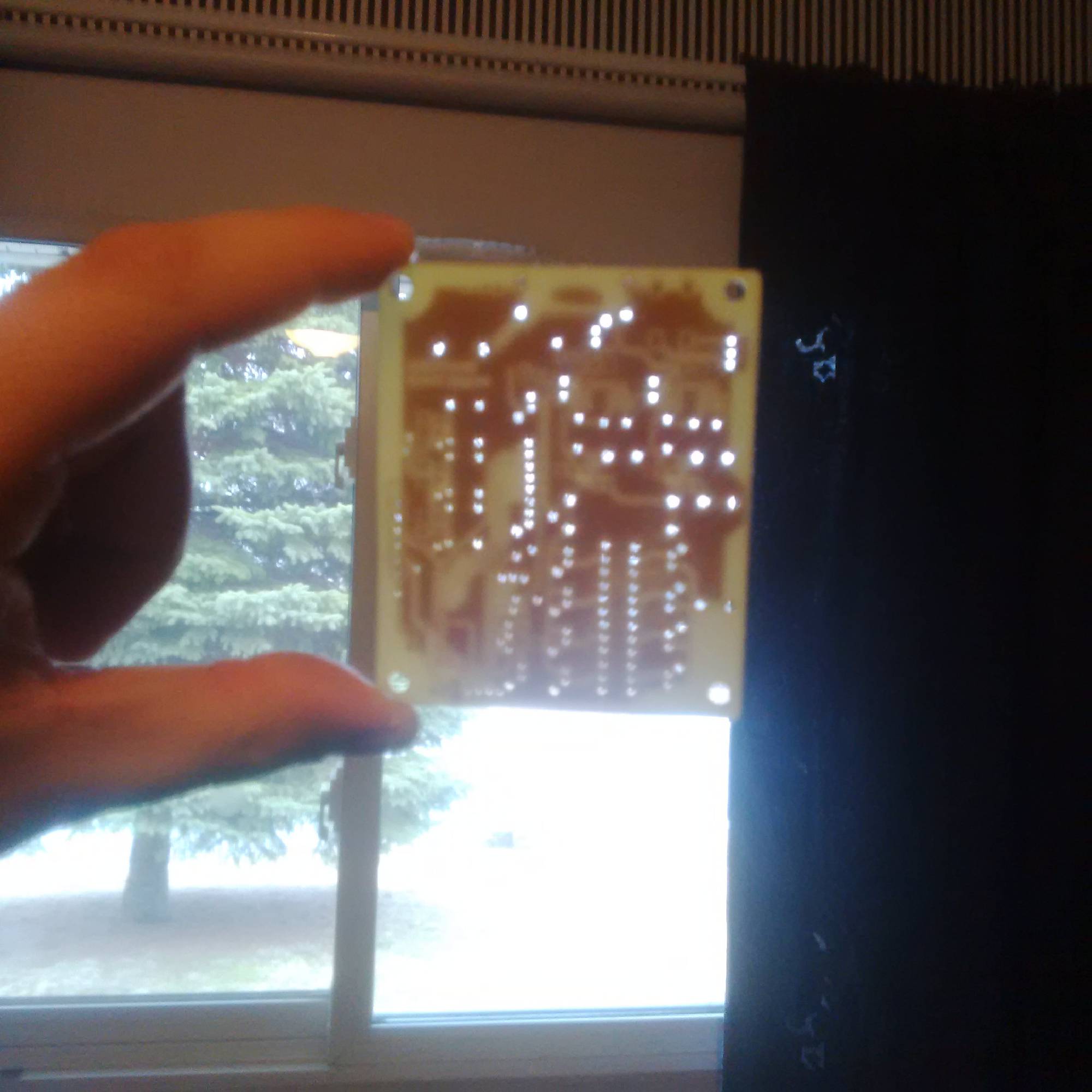
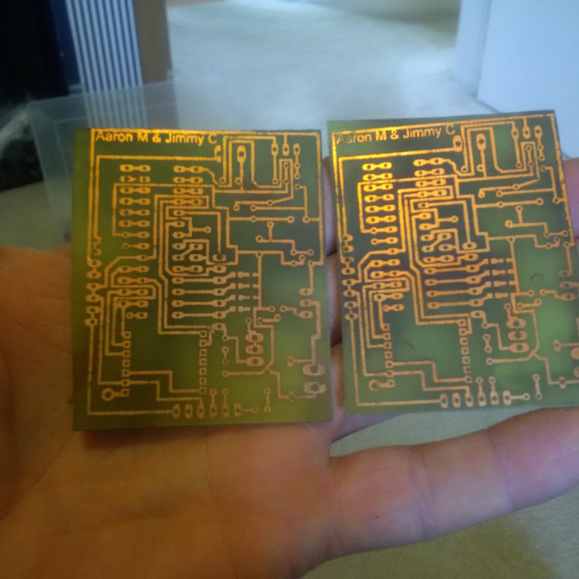
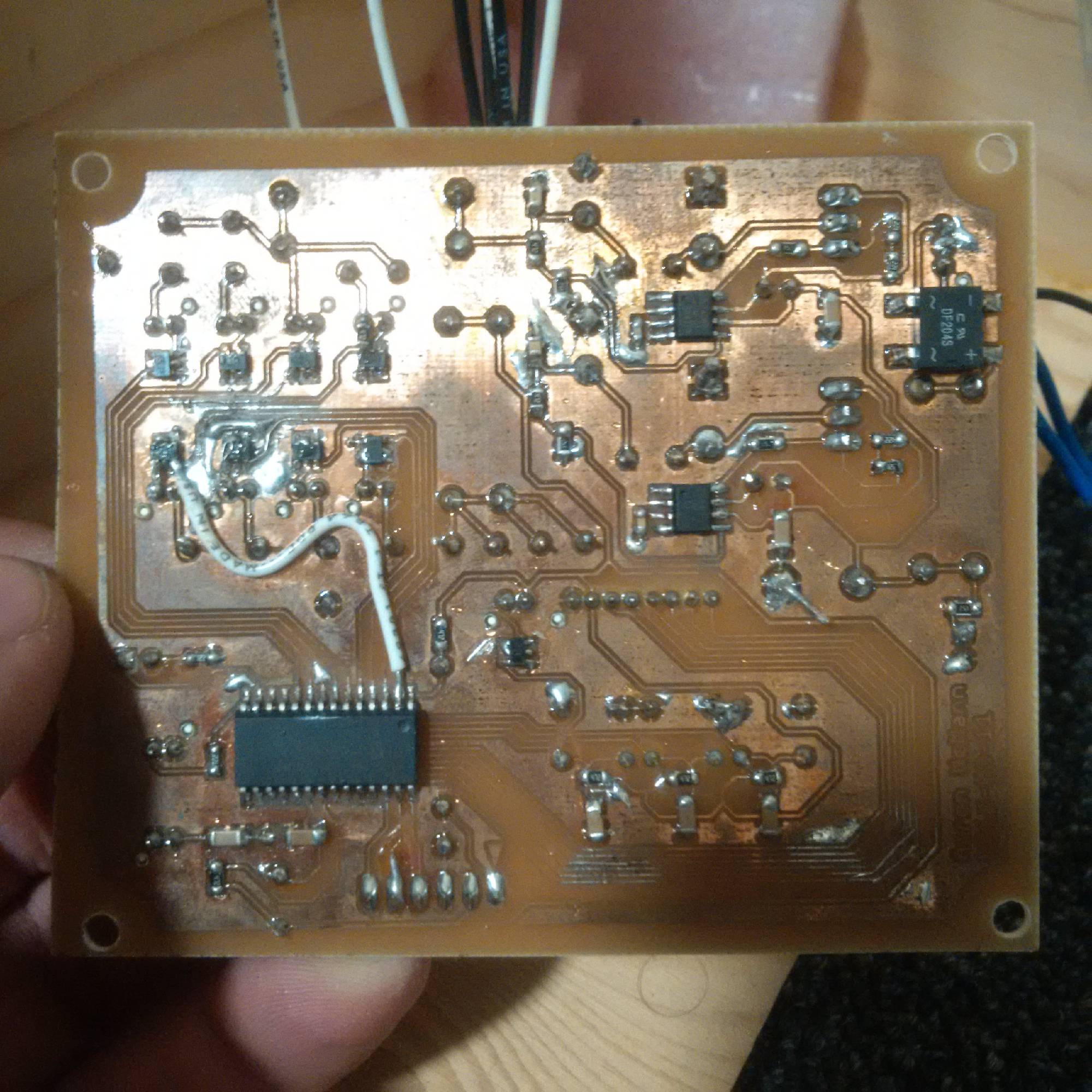
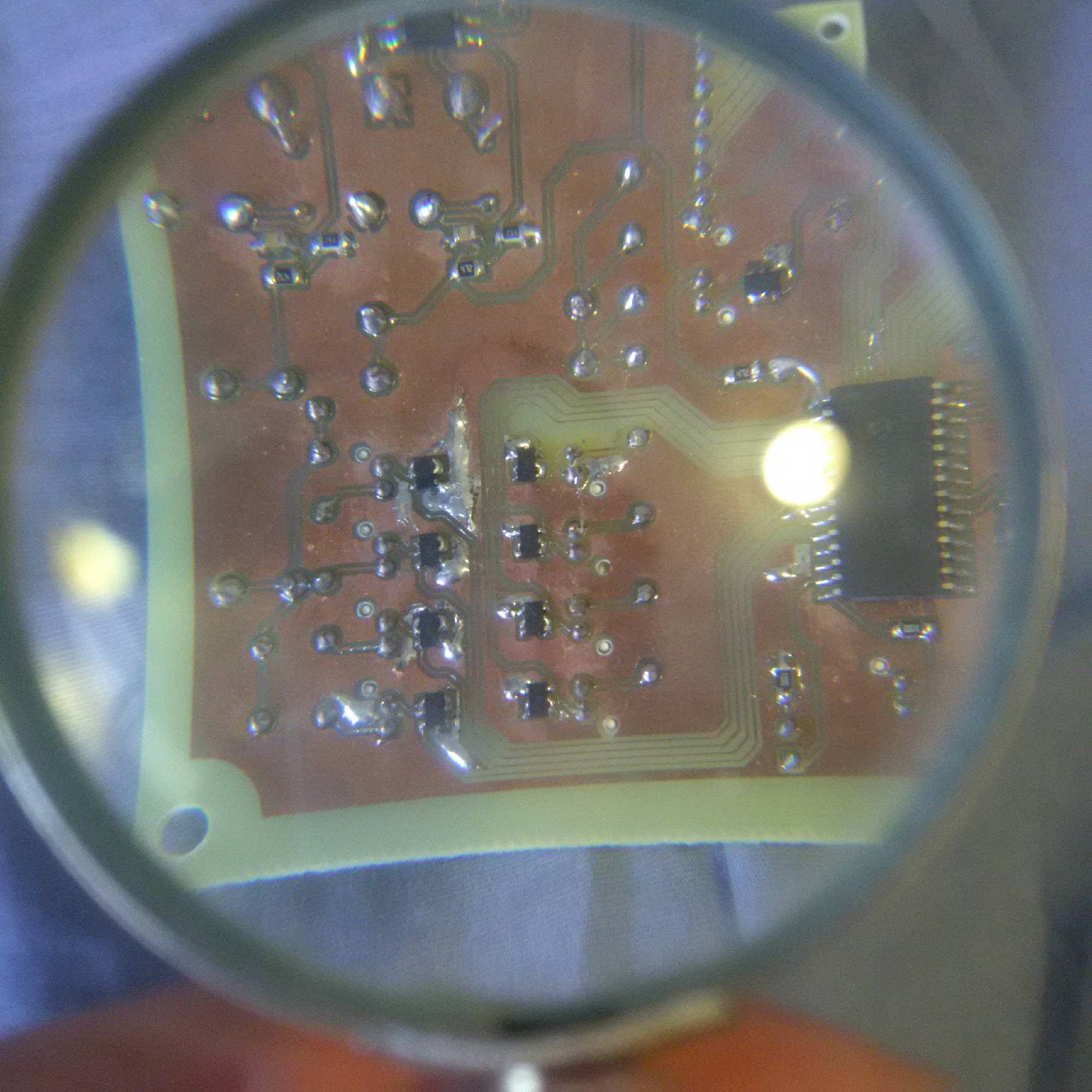
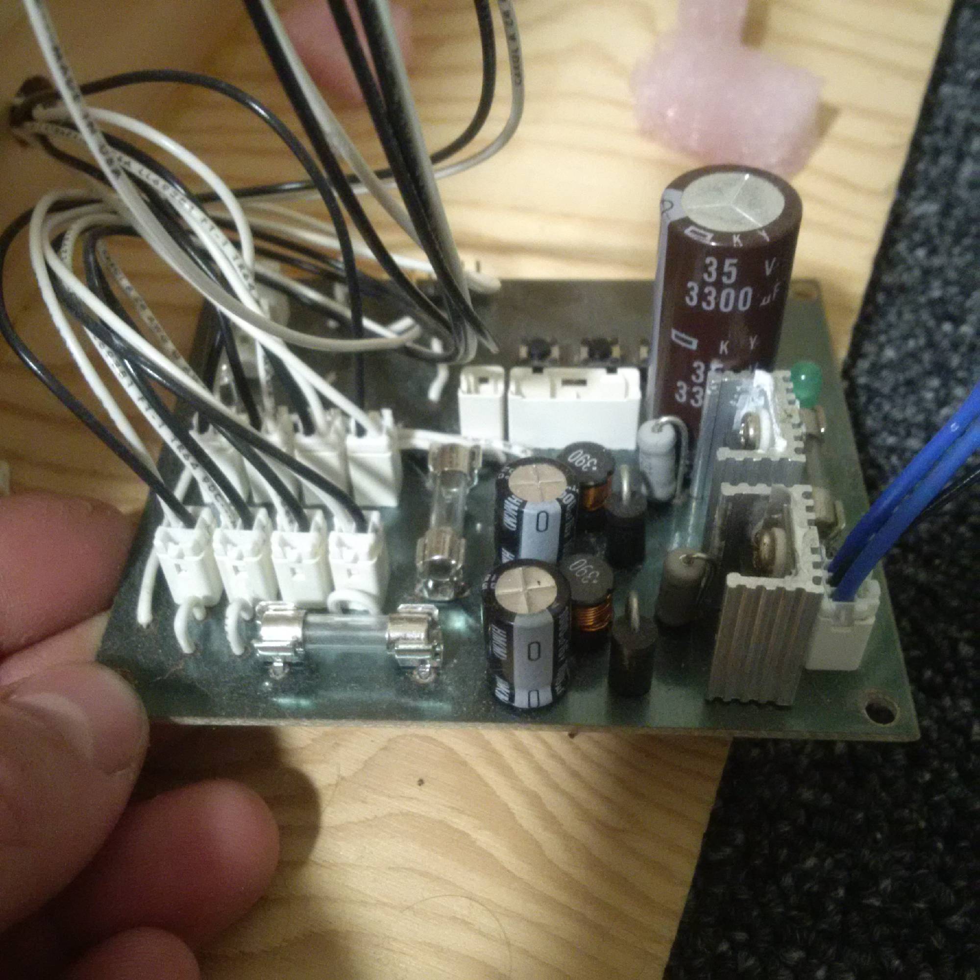
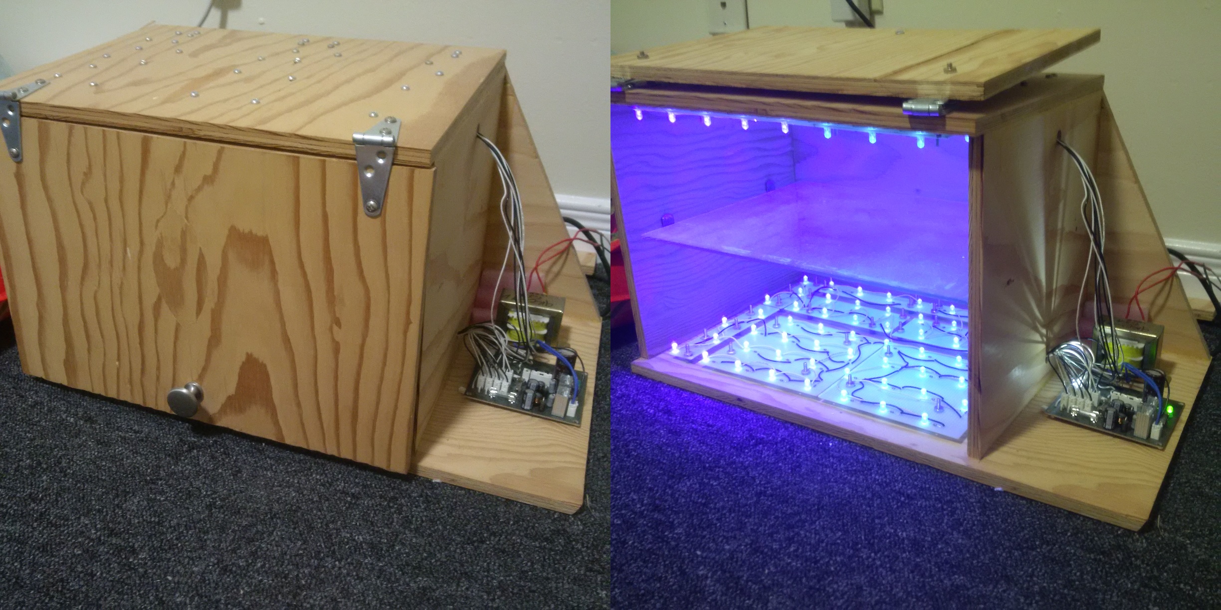
Being able to make your own PCBs is an incredible ability.  It definitely beats point-to-point soldering on a perf-board, and it's a precursor to learning efficient PCB layout, SMT work, and reflow soldering.  Needless to say, this is a must-have for the serious electronics enthusiast!

As I said on the page about my CNC milling machine, electronics is my passion. I didn't like the work that came with point-to-point soldering on a perfboard, so I started out with the iron-on method of making PCBs. This method works, but produces low quality PCBs, and issues are abundant because of the amount of manual labour involved. Furthermore, when you start looking for work, you have no concept of PCB design. To name a few concepts, component placement and selection, PCB size, and the number of drill holes are just a few of the topics, without talking in depth about trace width/orientation with regards to noise.


One feature is seperately controlled top and bottom UV LEDs, for manufacturing single/dual sided PCBs, and both the top and bottom are segmented into four different independent sections, allowing a wide range of sizes up to a maximum of 13.5"x10" without using any unnecessary power. Any PCBs larger than that will have to be professionally made, or designed into multiple smaller PCBs.

Another feature is an LCD screen (not shown above) with adjustable backlight.  This is useful for showing which LED sections are chosen without exposing the operator to any UV.  The ability to adjust backlight brightness also reduces energy consumption.  Since the sun, compact fluorescent bulbs, and incandescent bulbs all output some minor amount of ultraviolet light, having them on while working could influence the results.  Therefore there is an ultra-bright white LED so the operator can see what they're doing in an otherwise dark room.  Lastly, there are 2 power supply circuits for increased efficiency.  The bottom LEDs are on a seperate power supply so that if only single sided PCBs are being made, the bottom supply can be turned off, and even more power can be conserved.


This is what I use to make all of my PCBs now.  There can be any number of issues with the iron-on method such as broken traces or shorted traces, and a ground plane is almost never an option.  Dual sided PCBs were extremely difficult... but not anymore.

Oh and in case you're wondering, I always document everything in my lab logbook.

When I write it down, I can prove I did it; and if I did it, you can bet I wrote it down.